Semiconductor 3D Packaging
We need bigger and faster devices to manage more complex and larger amounts of data. As data evolves, the amount of data we process is growing rapidly, especially with digitization and the rise of digital twins. Semiconductor-based computing systems are essential in meeting these demands. The ability to meet compute requirements depends on available technology, the cost of development, power consumption, and thermal management solutions.
Different applications have varying needs: some require small, low-power devices, while others need large, energy-efficient semiconductor devices. Data centers struggle to manage energy use and cooling for their systems..
As computing moves to multicore and neural processing, some parts of neural processing are advancing faster than traditional semiconductor devices, which are limited by Moore’s Law. Moore’s Law is facing limits as devices get smaller and more complex, leading to higher costs and production difficulties.
Packaging of Silicon Chips
Silicon chips are composed of a silicon die, which is typically housed in a package that connects the die’s pads to the package’s external pads. Over the years, this packaging technology has evolved significantly.
Initially, silicon chips were packaged in dual inline packages (DIP) or quad flat packages (QFP), with connections between the die and the package substrate created through a process known as wire bonding. Early microprocessors and microcontrollers mainly used these formats, with materials like plastic or ceramic.
In the early days of wire-bonded packaging, a popular trend was the use of multichip modules (MCMs), which involved assembling multiple silicon dies on a single substrate package. This approach was especially valuable for high-performance applications like mainframes, compact systems, and high-reliability systems, such as those used in the military. MCMs offered advantages including low-capacitance, high-speed interconnects between dies, reduced power dissipation, enhanced reliability, and a compact form factor.
However, as silicon technology advanced, enabling higher integration and modern design styles, many multi-die functions were consolidated onto a single die. This shift resulted in more power-efficient, faster, and even more compact designs, leading to a gradual decline in the use of wire-bonded MCMs.

Wire bonded DIP/QFP package. By Mister rf – Own work, CC BY-SA 4.0, https://commons.wikimedia.org/w/index.php?curid=97847480
As logic density improved, designs expanded, increasing the number of I/O connections. From the early 16-pin DIP packages, I/O counts grew to over 100 and even 400 pins. This created two challenges: the density of pads on the design edges became higher, with some designs requiring staggered pads in two rows. This pushed the limits of edge-arranged pins in QFP packages, leading to the development of packages with pins arranged in a grid on the bottom surface. These new formats include Pin Grid Array (PGA), Ball Grid Array (BGA), and Land Grid Array (LGA) packaging.
With the rise of grid array packaging and high I/O density, wire-bonded packages became more challenging to design. The assembly process grew more prone to defects and costs rose, as maintaining adequate spacing and controlling parasitic effects became difficult due to the long wire lengths. The solution was flip-chip packaging, where the die is flipped upside down so the active area and pads face downwards, directly contacting bumps on the package.
Flip-chip packaging requires additional steps before assembly. First, wafers undergo passivation to protect against damage. Then, bumps—either spherical metal balls or copper pillars—are attached to allow the die to connect with the substrate. The gap between the silicon die and the substrate is then filled with an underfill material to ensure stability and reliability.


MCM Packaging Innovation
With the advent of flip-chip technology and increasing demands for power reduction, speed improvements, and miniaturization, the need for greater integration in system design has become essential. Modern systems also require more heterogeneous components, each sourced from different fabs and manufacturers. For instance, an image sensor camera includes a CMOS image sensor, an image processing chip, DRAM, and flash storage—each from distinct process technologies and often different vendors. Similarly, an integrated microcontroller subsystem combines the CPU, DRAM, flash, and PMIC chips into a single, compact, and cost-effective package.
One key advancement in Multi-Chip Module (MCM) packaging is the vertical stacking of dies. In this configuration, there are no direct physical connections between the dies; all connections are managed through the substrate.

IBM MCM package – Eric de Perfecto et. al.

(a) System in Package technology. (b) Package on Package technology
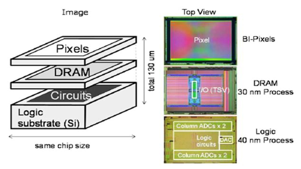
A key feature of multichip modules (MCMs) is that interconnections between dies, as well as die-to-package connections, are achieved using I/O pads, typically with standard pitch. Die-to-die connections often result in lower impedance than on-board connections, which enhances performance. These packaging solutions prioritize compact design, lower power consumption, and higher I/O speeds. Another essential aspect of MCMs is functional diversification. Many systems require compact designs with components from different process technologies and fabs. For example, image sensors incorporate various semiconductor components: an optical CMOS sensor with a detector and pixel array, plus DRAM for pixel storage. Each component demands different technologies, and their interconnection is facilitated by Through Silicon Via (TSV) technology.

The 3D image sensors for smartphones. The components are made in different technologies and assembled. A REVIEW OF THE RECENT DEVELOPMENTS IN THE FABRICATION PROCESSES OF CMOS IMAGE SENSORS FOR SMARTPHONES
Through Silicon Via (TSV) Technology
TSV technology enables silicon die stacking in image sensors by connecting two vertically stacked dies. The top wafer is aligned and processed to create vias that extends to its backside, which is thinned to 10 microns or less, allowing a connection to the metal layer of the second wafer. In earlier multi-die packages, connections were made solely through the substrate. TSV, however, has electrical and physical characteristics similar to silicon-based integrated circuits, achieving higher density, speed, and lower power consumption compared to package-level connections.
TSV fabrication supports both 3D devices, where multiple dies are stacked vertically, and 2.5D devices, where components are placed side-by-side and interconnected via a silicon interposer. This process typically occurs in a wafer fab.
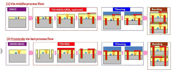
The TSV formation process can occur during the Front End of Line (FEOL), where lower metal layers are processed. Here, we outline the “via-middle” process, which builds TSVs just after transistor etching:
- Process the base layers, etching in active transistors.
- Etch openings for the TSVs using the Bosch cycling etch process.
- Passivate the vias and deposit copper for metallization.
- Complete Back End of Line (BEOL) metallization, applying the Redistribution Layer (RDL).
- Place the wafer on a carrier and thin it to expose the backside of the vias.
- Dice the wafer and attach it to the next die in the stack.
- Repeat the process for each die in the 3D stack.

Implementation of Memory Stacking on Logic Controller. Shang-Chun Chen et. al. VLSI-TSA 2016.
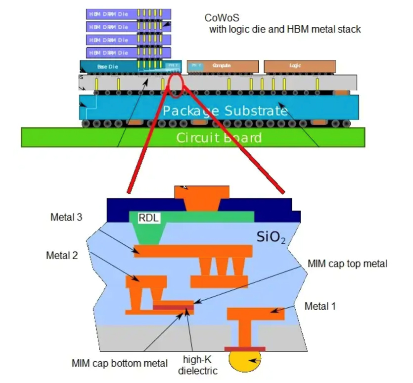
The commercially available process for 3D packaging is TSMC’s Chip-on-Wafer-on-Substrate (CoWoS) process. In this process, stacked devices are attached to a packaged substrate to form the final device. If the design requires, multiple devices can be attached to a base wafer, which lacks active devices and is referred to as a silicon interposer. This interposer, when it only contains metallization, is known as a silicon-interposer. While the chips can be fabricated in advanced nodes such as 7nm or 3nm, the base wafer typically uses larger geometry nodes, such as 45nm or 55nm, to handle the metal interconnects.

CoWoS Technology. TSMC Technology Forum 2020
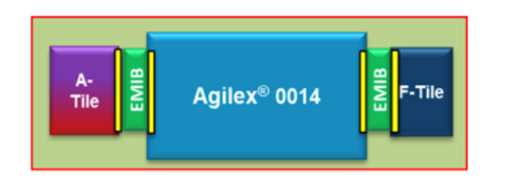
As silicon interposers grow larger, designing and achieving high yield becomes increasingly challenging. An alternative solution, developed by Intel, is the Embedded Multi-die Interconnect Bridge (EMIB). This packaging technology embeds a silicon strip into the package to establish die-to-die connections. Dies with direct I/O connections are linked to the package pins. While EMIB reduces the need for large silicon interposers, it requires advanced packaging technology.


Intel EMIB technology. Ability to connect multiple custom dies with silicon bridge.
The advent of TSV, die stacking, and interposers has greatly enhanced the ability to connect multiple dies, improving power, performance, and density compared to traditional PCBs. This enables the development of systems with more heterogeneous die components. However, to fully realize these innovations, there must be standards, frameworks, and commercial agreements facilitating the exchange of dies, or ‘chiplets,’ between companies, fabs, and CAD tool vendors. This exchange should function similarly to the IP core business, which has significantly accelerated chip development. As the chiplet business evolves, system companies can create more integrated and differentiated products. Beyond IP solutions, modern technologies are needed to support this growth. We will discuss the standards currently under development and those still needed to sustain the rapid growth of the electronics industry.

